Two-channel 125 MSPS ADC board
The schematic and layout are complete for a two-channel, 14-bit, 125 MSPS data acquisition board. ERC and DRC report no errors. The board has not been fabricated; the results are simulations and calculations.
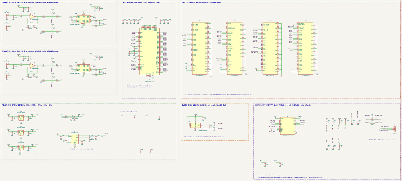
An Analog Devices AD9648 samples current and voltage signals and sends them to a Digilent Nexys Video FPGA board through an FMC connector. Its 16 LVDS pairs run at 250 Mb/s each. I chose this interface to leave more timing margin than the faster ADC options.
The design is open source on GitHub. The hardware files use the CERN-OHL-S 2.0 license, the code uses the MIT license and the documents use CC BY 4.0. The ai-context folder holds the prompts, design rules, workflow and Claude skill that I used to design the board with AI tools.
Analog input chain
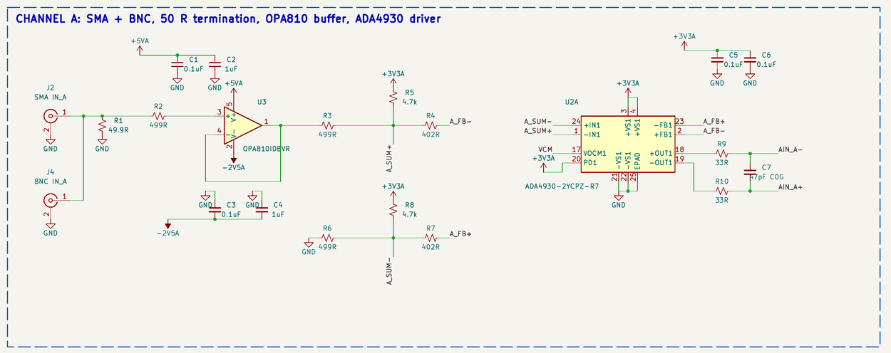
Each channel has an SMA connector and a BNC connector in parallel. Both connect to one 49.9 Ω terminator, so the input load is 50 Ω. Use only one connector on each channel at a time. The input range is ±1 V.
A 499 Ω resistor connects the input to an OPA810 buffer. The buffer isolates the connector from the bias current of the next stage. Without the buffer, the next stage put 28 mV back onto the input. One half of an ADA4930-2 fully differential amplifier then makes the signal differential and sets its common-mode voltage to the 0.9 V of the ADC. A 33 Ω and 47 pF filter is at the ADC pins.
One channel was simulated in LTspice with the vendor models of the OPA810 and the ADA4930. The table compares the results with the targets.
| Check | Result | Target |
|---|---|---|
| Gain, connector to ADC | 0.779 V/V (−2.17 dB) | Calibrate on each channel |
| Flatness, DC to 1 MHz | 0.09 % | ±1 % |
| −3 dB bandwidth | 50.1 MHz | 20 MHz or more |
| Delay, connector zero crossing to ADC zero crossing | 6.8 ns | 25 ns or less |
| Settling to 0.1 % after a 3.2 V step | 14.6 ns | |
| Recovery after a −2 V overload | 31 ns, to within 0.78 mV | |
| Driver noise at the ADC, DC to 20 MHz | 31.6 µV rms | |
| Total noise with the ADC, referred to the connector | approximately 105 µV rms (calculated) | 300 µV rms or less |
| ADC pin voltage for ±5 V at the connector | 0.20 V to 1.60 V | −0.3 V to 2.0 V |
Protection resistor. The OPA810 input accepts 10 mA continuous. With the first value of 100 Ω, a −5 V fault at the connector sends approximately 20 mA into the input clamp. The revised design uses 499 Ω. The same fault now sends approximately 4 mA. This estimate uses the negative clamp voltage of approximately -3 V on the -2.5 V supply.
\[ I_{\mathrm{clamp}} \approx \frac{|-5-(-3)|}{499} = 4.0\,\mathrm{mA} \]
Terminator rating. A ±5 V fault into 49.9 Ω is 0.5 W. An 0402 resistor survives only approximately ±1.8 V continuous. The design specifies a 1206 resistor rated at 0.25 W. Its nominal power limit corresponds to approximately ±3.5 V continuous, before temperature derating.
\[ P_R = \frac{V_{\mathrm{in}}^2}{R} = \frac{5^2}{49.9} \approx 0.50\,\mathrm{W} \]
\[ |V_{\mathrm{in,max}}| = \sqrt{P_{\mathrm{rated}}R} = \sqrt{0.25\times49.9} \approx 3.53\,\mathrm{V} \]
Noise. The SNR of the AD9648 is approximately 74.5 dBFS. For a 2 Vpp span, this is 133 µV rms in the 62.5 MHz Nyquist band, or 96 µV rms in 20 MHz referred to the connector. The root-sum-square with the 40.5 µV driver noise is approximately 105 µV rms. This estimate assumes uncorrelated noise sources and a flat ADC noise density over the Nyquist band.
\[ v_{n,\mathrm{in}} = \sqrt{v_{n,\mathrm{ADC,in}}^2 + v_{n,\mathrm{driver,in}}^2} \]
\[ v_{n,\mathrm{in}} \approx \sqrt{96^2+40.5^2} = 104.2\,\mathrm{\mu V_{rms}} \]
Anti-aliasing. The single RC pole gives −6.4 dB at 62.5 MHz and −30.6 dB at 187.5 MHz. This filter is weak. It is acceptable because the external sensor limits the bandwidth. If the sensor bandwidth is more than 60 MHz, the next revision needs a second-order filter.
Power, clock and control
The board gets 3.3 V and 12 V from the FMC connector. Two TPS7A20 LDOs make the 1.8 V analog and 1.8 V digital rails for the ADC. A TLV767 LDO makes +5 V from 12 V for the buffers. An LM27761 charge pump makes −2.5 V. A ferrite and a 10 µF capacitor filter the 3.3 V rail for the amplifiers and the clock. The board takes approximately 0.37 A from the FMC 3.3 V rail. The FMC limit is 3 A.
A Si531 oscillator supplies a 125 MHz LVDS clock to the ADC through 0.1 µF coupling capacitors.
The FPGA control pins operate at 2.5 V. The absolute maximum of the ADC control pins is 2.0 V. An SN74AXC4T774 translator connects the SPI bus between the two voltages. For a read, the FPGA changes the direction of the SDIO line. Pull resistors hold each control line at a safe level when the FPGA is not configured.
The AD9648 starts in 1.8 V CMOS output mode. In this mode, it drives CMOS levels into the LVDS inputs of the FPGA. A 4.7 kΩ pull-up against the 26 kΩ internal pull-down holds the OEB pin at 1.52 V. The minimum high level is 1.22 V, so the outputs stay off at power-up. The firmware selects LVDS over SPI and then enables the outputs.
PCB layout
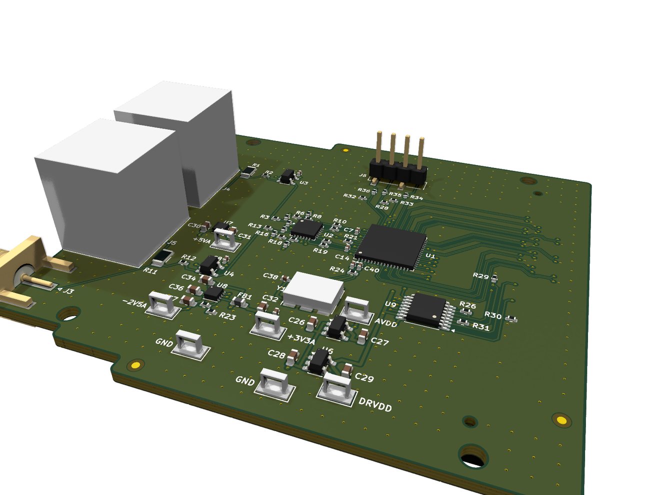
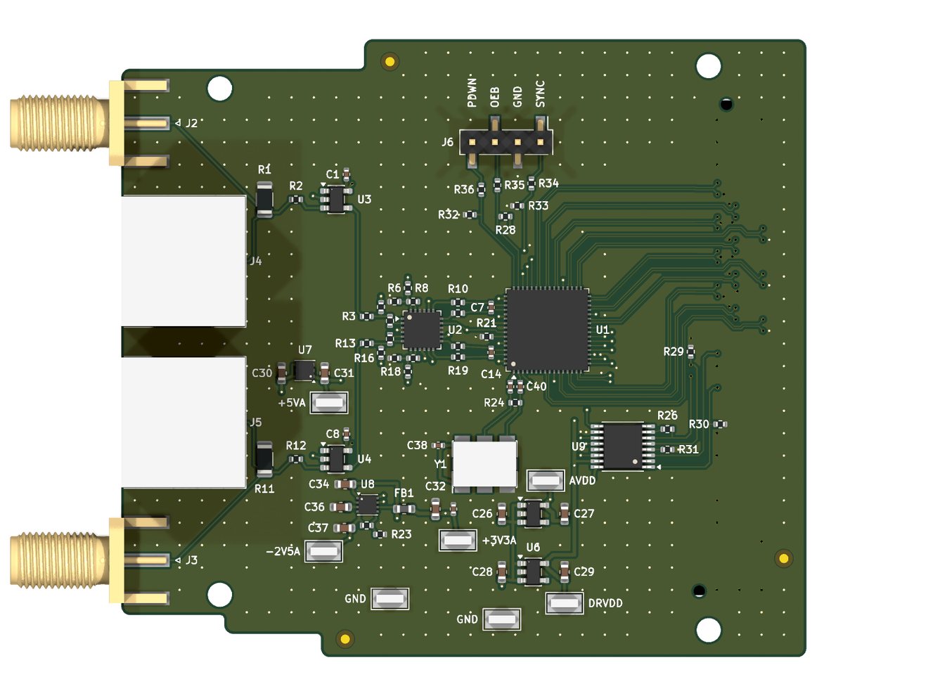
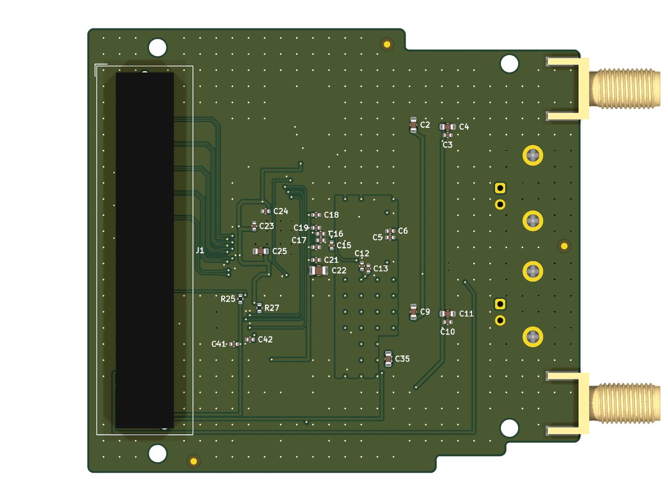
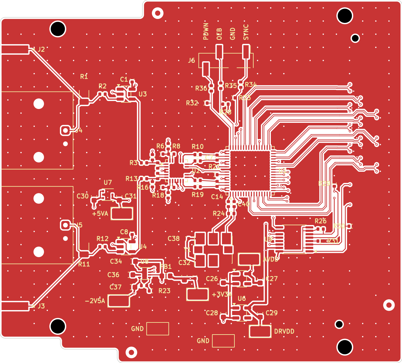
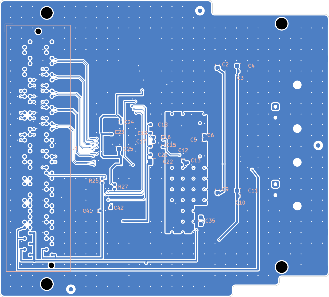
The board uses the VITA 57.1 single-width outline, 76.5 × 69 mm. It has four layers. Both inner layers are solid ground, so each signal trace has a continuous return path. The ground has no split. The placement keeps the analog inputs on the left, the ADC in the middle, and the LVDS lines and the FMC connector on the right.
Python scripts in KiCad 10 place the parts and draw each trace. The routing is scripted without an autorouter. After a change, the scripts run again and rebuild the board.
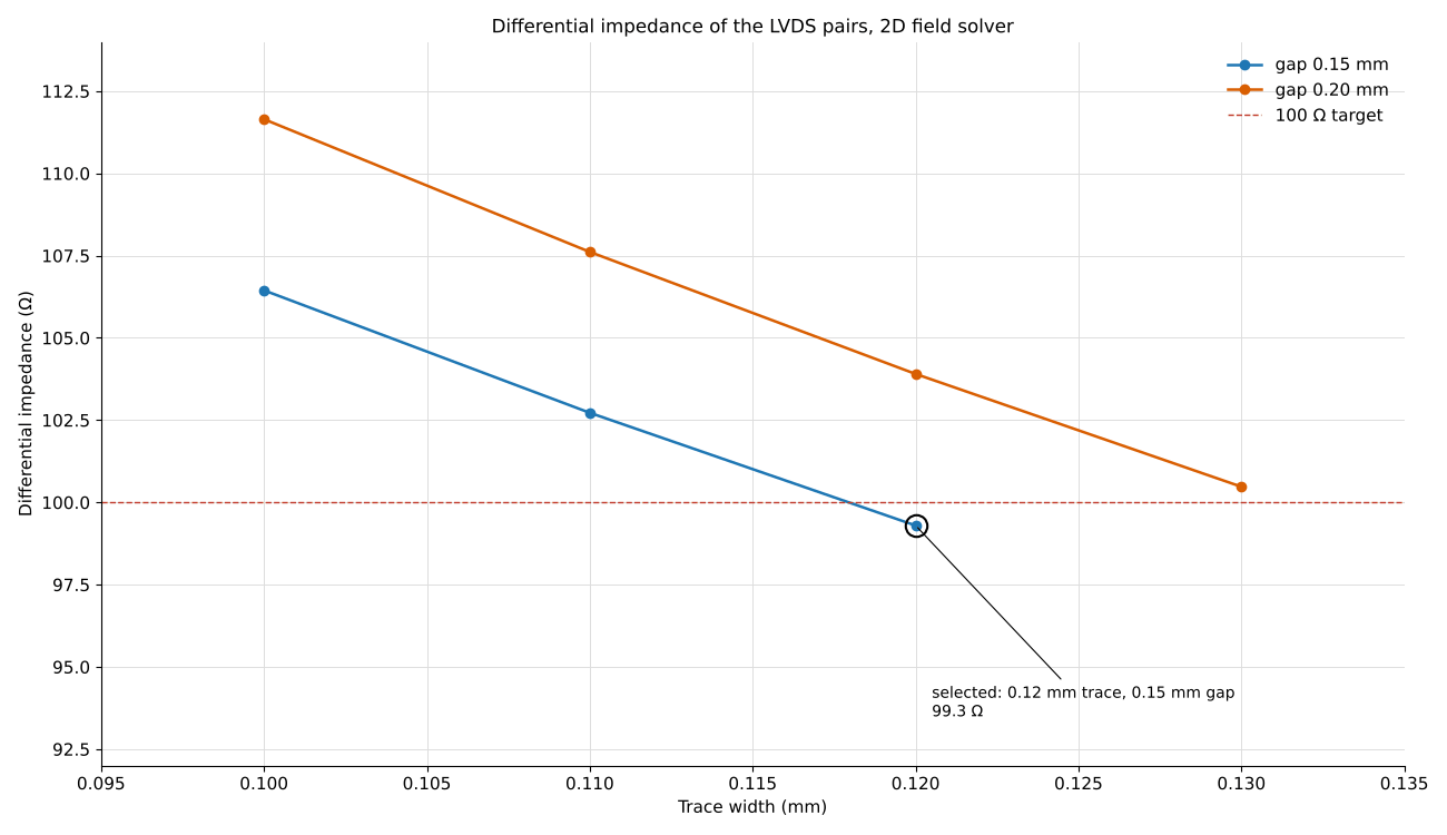
A 2D field solver sets the trace widths. Its results agree with the Hammerstad-Jensen equations within approximately 2 %.
| Structure | Geometry | Result |
|---|---|---|
| LVDS pair over ground | 0.12 mm trace, 0.15 mm gap | approximately 100 Ω differential |
| Analog input trace | 0.16 mm trace | approximately 50 Ω |
| Ground pour next to a pair | 0.25 mm gap or more | less than 0.5 % change in impedance |
| Space between two pairs | 0.25 mm | approximately 0.4 % crosstalk |
The LVDS data lines are 17.5 mm to 38.1 mm long. The clock line (DCO) is 27.2 mm long. The difference gives −57 ps to +63 ps of skew, which is inside the receiver timing margin. The two lines of each pair match within 0.57 mm.
Via transition simulation
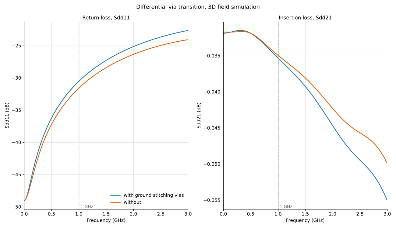
The LVDS pairs change from the bottom layer to the top layer near the FMC connector. An openEMS model, using a 3D FDTD solver, represents this via transition. The model has two signal vias 1.27 mm apart. The simulation compares the transition with and without ground vias next to the signal vias.
1 GHz is approximately the highest frequency in a 0.3 ns LVDS edge. At 1 GHz, the transition reflects approximately 3 % (−30.5 dB) and loses 0.04 dB. The ground vias change the reflection by only approximately 1 dB, because the partner trace carries most of the return current. A ground via next to each signal via provides the common-mode return.
FPGA design
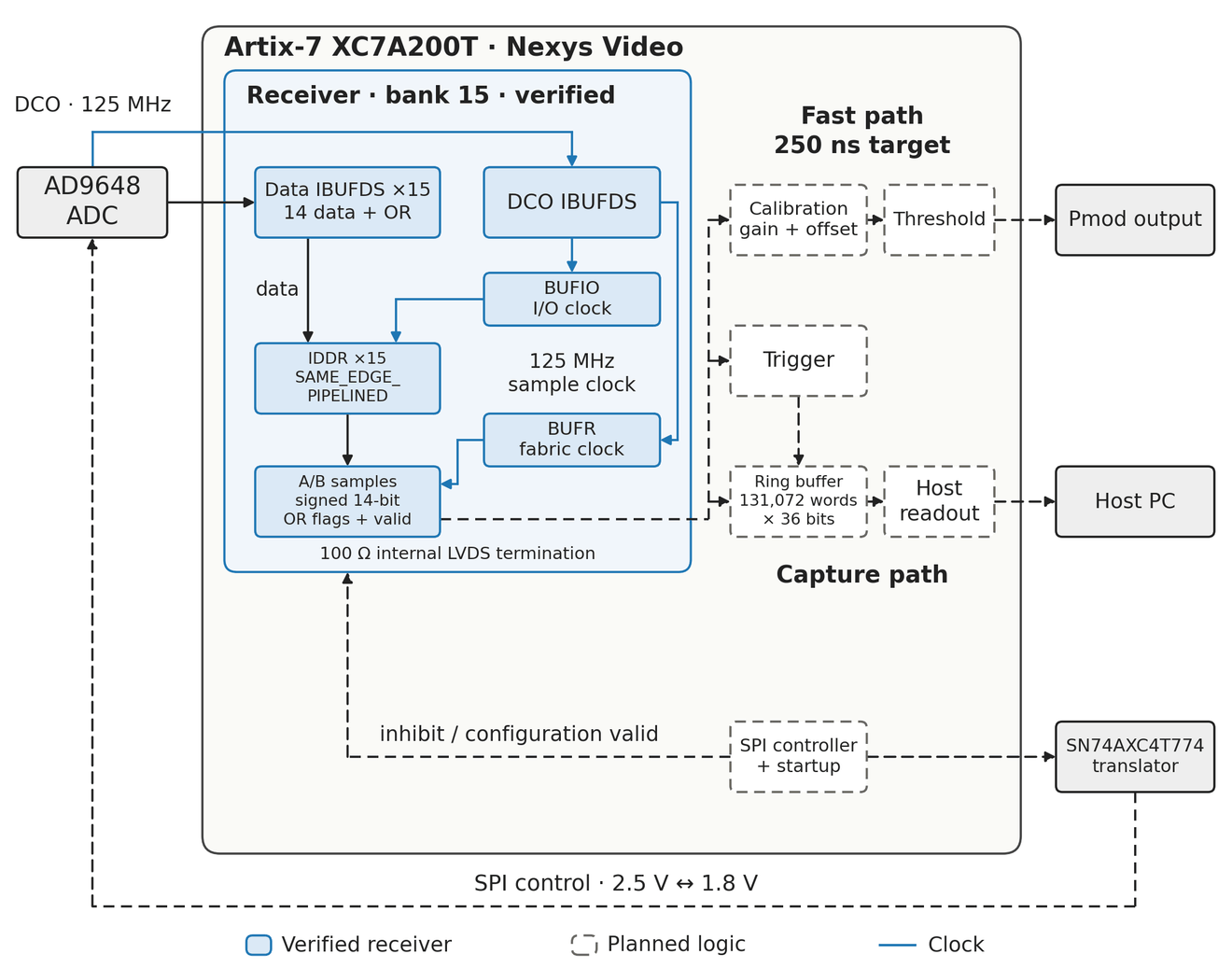
The FPGA design has two paths after the receiver. The fast path calibrates each sample, compares it with a threshold and drives an output pin. The capture path keeps a record around a trigger and sends it to a host computer. An SPI controller configures the ADC before both paths start. The diagram shows the planned blocks. Only the receiver is written and verified.
Receiver: clocking and capture
The ADC output clock (DCO) is 125 MHz. It enters the FPGA on a clock-capable pin pair, through an IBUFDS buffer with the internal 100 Ω termination. A BUFIO buffer clocks the input registers of the 15 data lanes. A BUFR buffer clocks the fabric logic in the same clock region. This path has no MMCM, so the receiver does not wait for a PLL lock. The 14 data pairs, the overrange pair and DCO are all in bank 15, because a BUFIO clocks only the I/O of its own bank. The bank operates at VADJ = 2.5 V for the LVDS_25 inputs.
The ADC changes each data bit on both clock edges, so each lane carries 250 Mb/s. Each lane goes into an IDDR register in SAME_EDGE_PIPELINED mode. This mode gives the rising-edge bit and the falling-edge bit together on one rising edge. In interleaved mode, the rising-edge bits are channel A and the falling-edge bits are channel B. A separate simulation of the IDDR primitive confirmed which two bits it outputs together before receiver implementation.
For each 8 ns clock cycle, the receiver outputs one signed 14-bit sample for each channel, an overrange flag for each channel and a valid flag. Both samples come from the same sampling instant.
An asynchronous inhibit input clears the outputs at once. It also operates when the ADC clock is stopped. Two synchronizer flip-flops release the inhibit in the sample clock domain, and the valid flag comes on three clock cycles later. The firmware holds the inhibit until the SPI configuration is complete.
Receiver: verification and timing
A Vivado pin audit compared the 44 allocated package pins with the bank, pair and clock-capable properties of the XC7A200T. All 44 checks passed.
The testbench runs three copies of the receiver at the same time, with data-to-clock skews of −0.40 ns, +0.03 ns and +0.45 ns. Channel A sends zero, the full-scale values, walking ones, walking zeros and a ramp. Channel B sends an independent pseudo-random sequence. The two overrange flags use different patterns, so a swap of A and B gives an error. The testbench compares each output pair with the expected pair for the same sampling instant. It also applies 100 resets at different clock phases and stops the clock to check the inhibit. All three copies passed, with more than 970 comparisons each.
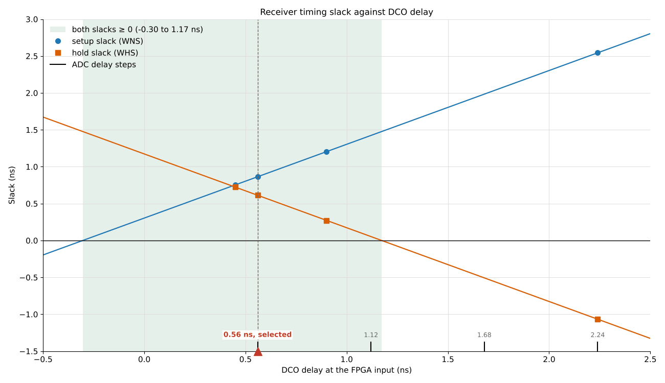
The timing constraints model the ADC as a virtual launch clock. The data-to-DCO skew is −0.20 ns to +0.25 ns from the datasheet, plus 0.10 ns for the board. Each data edge is checked against the next DCO edge of the same direction. Vivado placed and routed the receiver for the XC7A200T-1. The ADC can delay its DCO output in steps of 0.56 ns, and the default delay is 2.24 ns. Four delay settings were tested to find the timing window.
| DCO delay | Setup slack | Hold slack | Result |
|---|---|---|---|
| 2.24 ns (default) | 2.544 ns | −1.067 ns | Fails hold on all 15 lanes |
| 0.90 ns | 1.204 ns | 0.273 ns | Passes |
| 0.56 ns | 0.864 ns | 0.613 ns | Passes, selected |
| 0.45 ns | 0.754 ns | 0.723 ns | Passes |
The IBUFDS and BUFIO add approximately 3.2 ns of clock delay at the slow corner. The default 2.24 ns delay therefore moves the capture edge past the 4 ns data window. The slack changes linearly with the delay, and the valid window is approximately −0.3 ns to +1.17 ns. Only the 0.56 ns step is inside it. Another option is to keep 2.24 ns and add approximately 1.8 ns of IDELAYE2 delay on each data lane. That option needs an IDELAYCTRL and a 200 MHz reference clock, so it remains an option for lane trimming after the board is built.
The routed receiver uses 40 I/O pins, 15 IDDR registers, one BUFIO, one BUFR and 10 LUTs. DRC shows no errors.
Startup sequence
The ADC starts in CMOS output mode with its outputs off. The FPGA must set the bank voltage and configure the ADC before it accepts data. The SPI controller will do these steps in this sequence:
| Step | Action |
|---|---|
| 1 | Configure the FPGA. All control outputs go to their safe levels. |
| 2 | Disable VADJ, set it to 2.5 V, enable it and wait for it to become stable. |
| 3 | Make sure that the board rails are good. |
| 4 | Enable the SPI translator. |
| 5 | Write register 0x14 (LVDS ANSI, interleaved, two's complement) and 0x17 = 0x80 (0.56 ns DCO delay). Write 0xFF = 0x01 to transfer. |
| 6 | Write 0x101 bit 7 = 0 to enable the outputs, then 0xFF = 0x01. Wait for DCO, then release the receiver inhibit. |
The SPI bus is three-wire, at 10 MHz or less. For a read, the FPGA sends the 16-bit instruction, then releases SDIO and changes the translator direction before the first data bit. The FPGA and the translator must not drive SDIO at the same time.
Fast path and capture path (planned)
The first test of the fast path is one signed threshold decision on a Pmod pin. The latency target is 250 ns, from a zero crossing at the input connector to the FPGA output pin. The table shows the budget.
| Term | Allocation |
|---|---|
| Wait for the next sample | 8 ns |
| ADC, 16-cycle pipeline and output clock | 140 ns |
| Receiver, calibration, threshold and output register (4 cycles) | 32 ns |
| Analog input chain (6.8 ns in simulation) | 25 ns |
| FPGA output routing | 8 ns |
| Total | 213 ns (37 ns margin) |
Calibration applies a gain and an offset to each channel. The LTspice gain of 0.779 and offset of −0.86 mV show that both terms are necessary.
The capture path stores samples in a ring buffer and stops a set number of samples after the trigger. A 1 ms record at 125 MSPS is 125,000 sampling instants. An on-chip buffer of 131,072 words of 36 bits holds two 16-bit samples and four status bits for each instant. It uses 128 of the 365 block RAMs, which is 35 %. This is a resource calculation; the buffer has not been synthesized.
\[ N = f_s T = 125\times10^6\times10^{-3} = 125{,}000 \]
\[ N_{\mathrm{BRAM36}} = \frac{131{,}072}{1{,}024} = 128 \]
Each RAMB36 block supplies 1,024 words at 36 bits, so the proposed buffer uses 128 blocks, approximately 35 % of the device.
Two channels at 125 MSPS in 16-bit words make 500 MB/s. This rate is more than a 1 Gb/s link can send, so the host reads one complete record after each trigger. Capture stops while the host reads the record. The host link has not been selected yet.
\[ R_{\mathrm{data}} = 2\times125\times10^6\times\frac{16}{8} = 500\,\mathrm{MB/s} \]
The SPI controller, calibration, threshold output, capture buffer and host readout are not written yet.