48 V GaN inverter
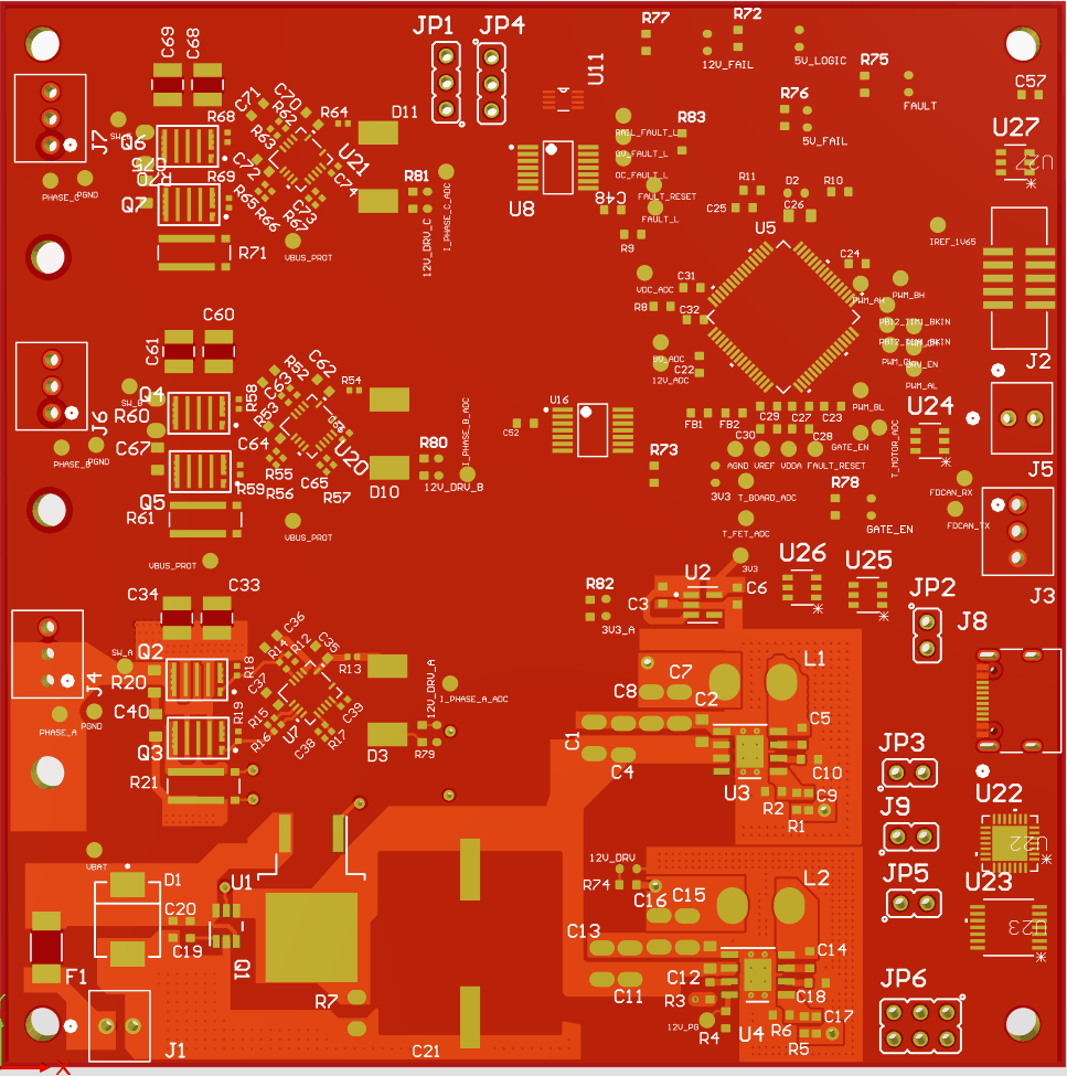
I completed the schematic for a 48 V three-phase GaN inverter, then stopped during the Rev A layout. The board was not fabricated or bench-tested.
The design takes 36 to 60 V and switches at 100 kHz under an STM32G474RET6 controller. The schematic has 238 components on a planned four-layer, 4 × 4 in board.
Power stage and gate drive
Each phase is a half-bridge of two Infineon IGC033S10S1 100 V CoolGaN FETs. One onsemi NCP51810 gate driver drives each half-bridge. The driver supply is 12 V, and the logic supply is 5 V. Each driver uses a bootstrap supply for the high-side FET.
I set the values below for the first power-up. The final dead time and gate resistor values were to come from double-pulse tests.
| Item | Value |
|---|---|
| Gate resistors | 2.2 Ω source, 1.0 Ω sink |
| Gate pull-down resistors | 10 kΩ |
| Dead-time resistor | 30.1 kΩ (approximately 30 ns hardware minimum) |
| Bootstrap diode | MBRS4201T3G, 200 V Schottky, with 4.7 Ω in series |
| Bootstrap capacitor | 220 nF |
| Snubber on each phase | 4.7 Ω and 1 nF |
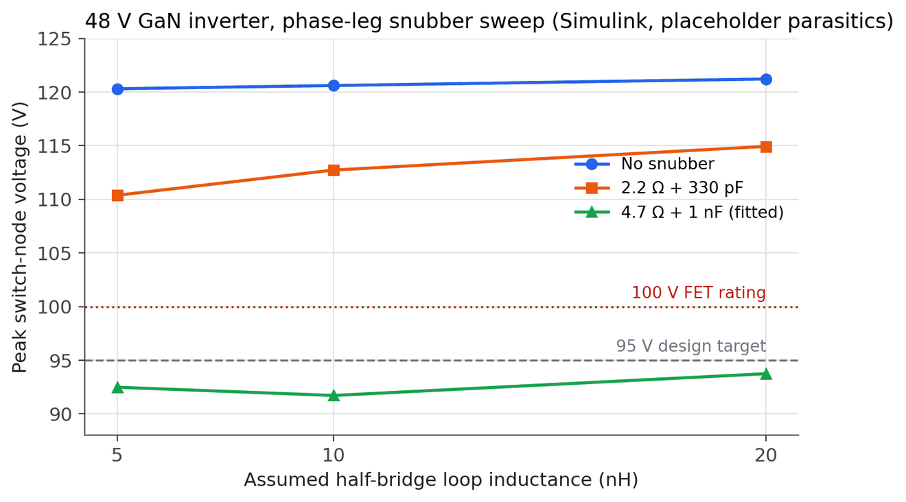
I compared three snubber options in a Simulink model of one phase leg, with a loop inductance of 5 nH, 10 nH and 20 nH. With the 4.7 Ω, 1 nF snubber, the switch-node peaks are 92.49 V, 91.72 V and 93.75 V. A 2.2 Ω, 330 pF snubber gives 110.38 V to 114.94 V. Without a snubber, the peaks are 120.31 V to 121.22 V. Only the 4.7 Ω, 1 nF snubber stays below the 95 V target. These inductance values are estimates. They do not come from the layout.
Sensing and protection
The current sense uses 10 mΩ four-terminal shunt resistors and INA240A1 amplifiers with a gain of 20. The sense range is ±5 A. TLV9024 comparators trip at ±6 A of phase current and at 68 V on the bus. A trip sets a fault latch. The latch output goes to the TIM1 break input of the STM32, and the bridge stops with no firmware action. In a simulation with an estimated delay model, the bridge stops 1.20 µs after the fault.
A 3 A fuse, an SMCJ64A TVS diode and an LM74700 ideal-diode controller protect the input. A 47 kΩ resistor discharges the bus from 60 V to 5 V in approximately 18 s. Rev A has no hot-swap stage, because the LM5060 controller had no stock. At 36 V input, the continuous output is limited to 22 V RMS line to line.
A thermal estimate gives approximately 1.7 W of total bridge loss. At 40 °C ambient, the junction temperature is approximately 60 °C. This estimate uses an assumed switching energy of 5 µJ and a thermal resistance of 40 °C/W. It is not a measured value.