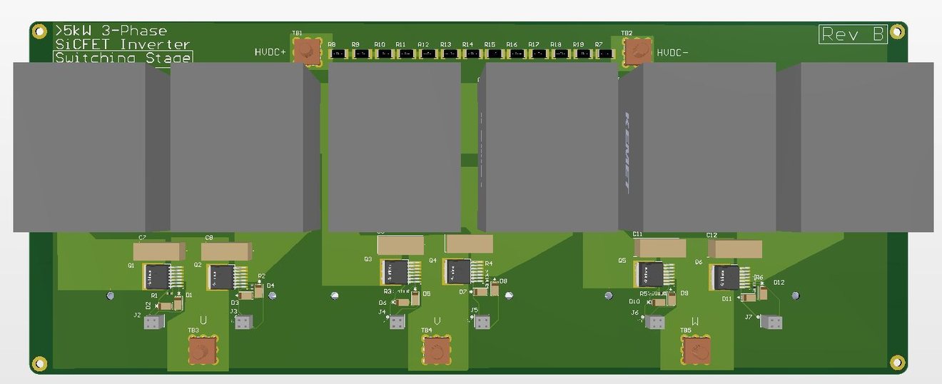
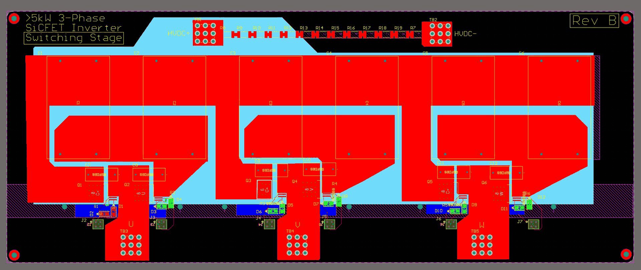
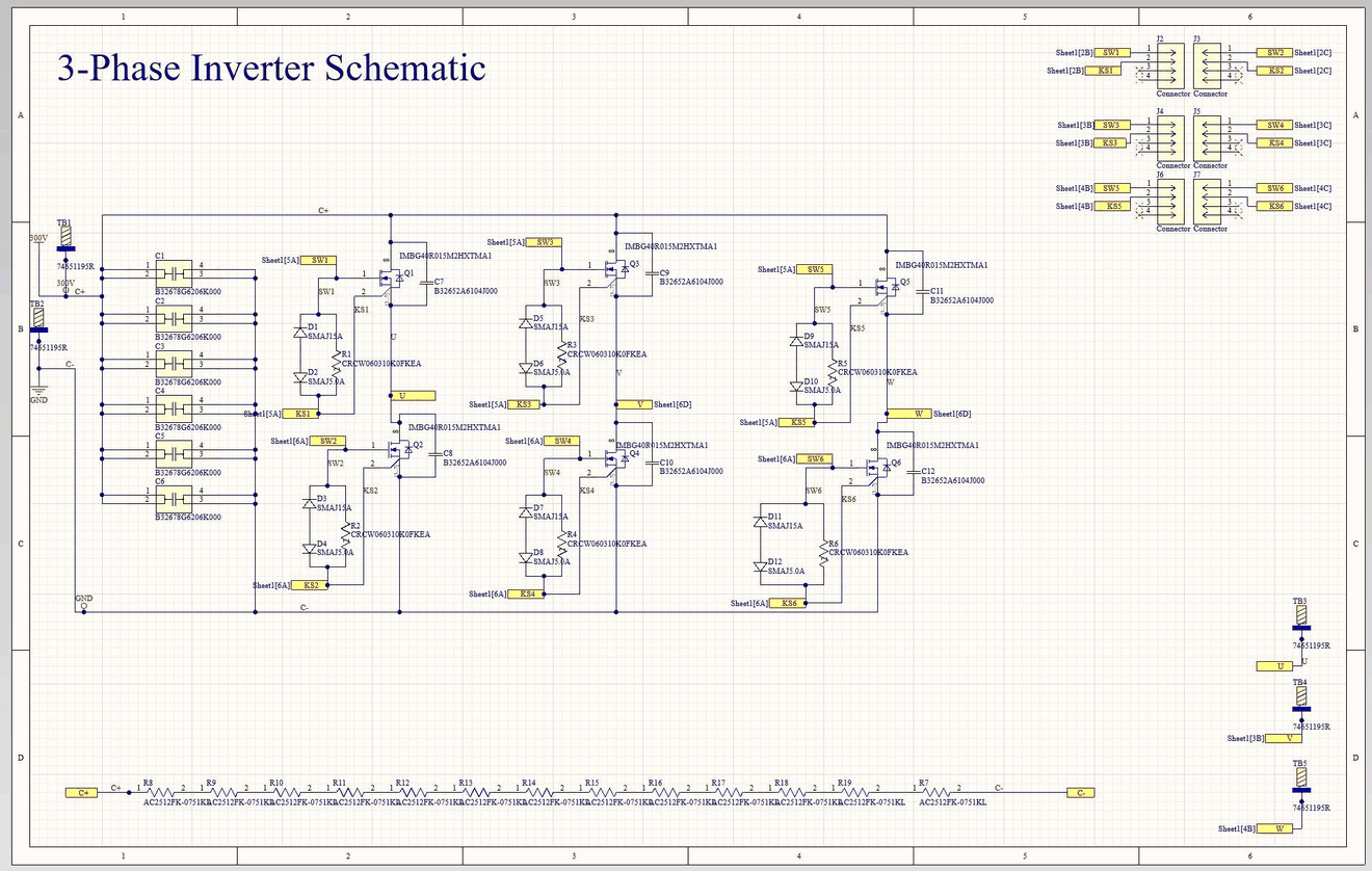
A three-phase silicon-carbide FET inverter designed in Altium for over 5 kW at 250 V. A discharge circuit keeps the bus safe to touch after disconnect.
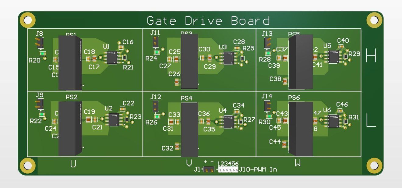
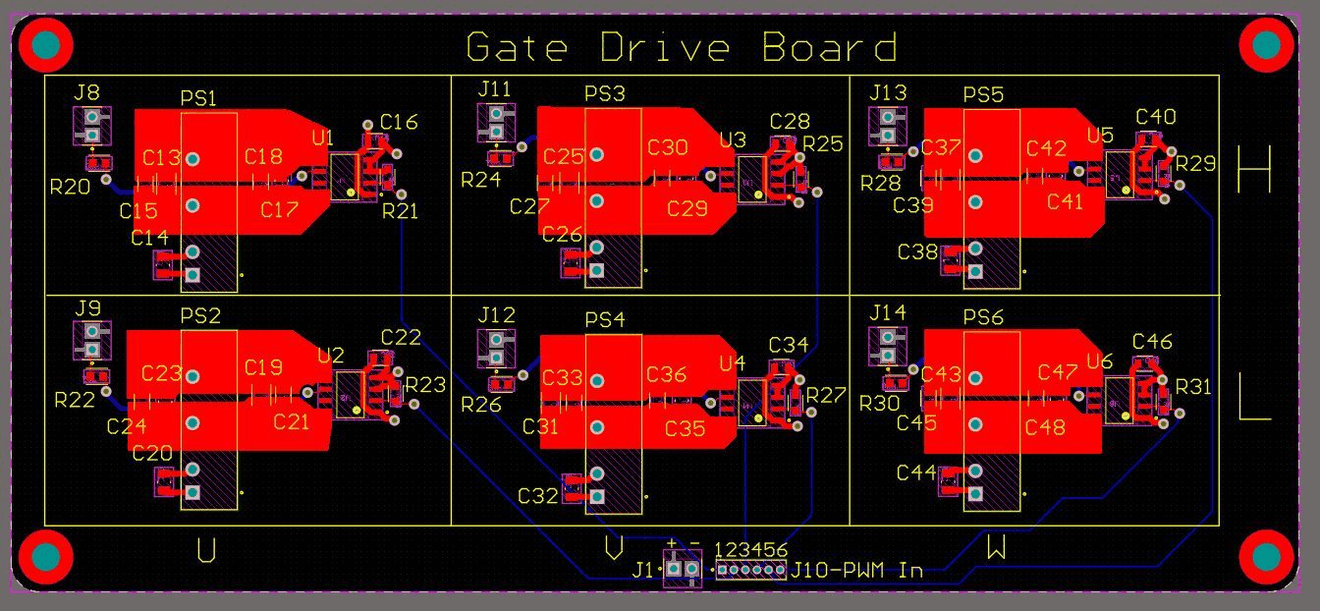
A separate isolated gate-drive board works with a range of high-power inverters. It isolates each gate with isolated driver ICs and isolated DC-DC modules that step 5 V up to 15 V.
Next up: PDN routing simulation in Altium's Power Analyzer, and an ESP32-S3 with a PCB antenna on the gate-drive board for motor-control testing and telemetry.
3D view of the Rev B switching stage: the three SiC half-bridges on heatsinks, with the U, V and W outputs along the bottom.Switching-stage layout, with wide copper pours carrying the high-voltage DC bus to each phase leg.Inverter schematic: three SiC half-bridges, their gate-drive connectors, and the resistor string that discharges the bus.3D view of the gate-drive board: six isolated channels, a high side and a low side for each of the U, V and W phases.Gate-drive board layout. Each channel has its own isolated DC-DC module and driver IC, split into separate isolated zones.