Isolated gate drive board
I designed a six-channel isolated gate-drive board in Altium. Rev E is the current design snapshot; the bench measurements below are from Rev D. The DRC reports predate the latest Rev E changes, and the board has no qualified operating range.
Each channel uses a TI UCC5310MCDR and a Murata MER1S0515SC to turn 5 V into a nominal isolated 15 V gate supply. The four-layer board accepts six 3.3 V PWM inputs. The external controller and power stage provide dead time, current protection and fault shutdown.
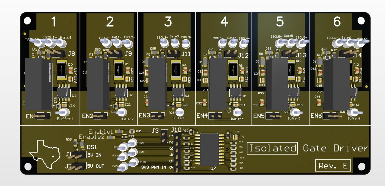
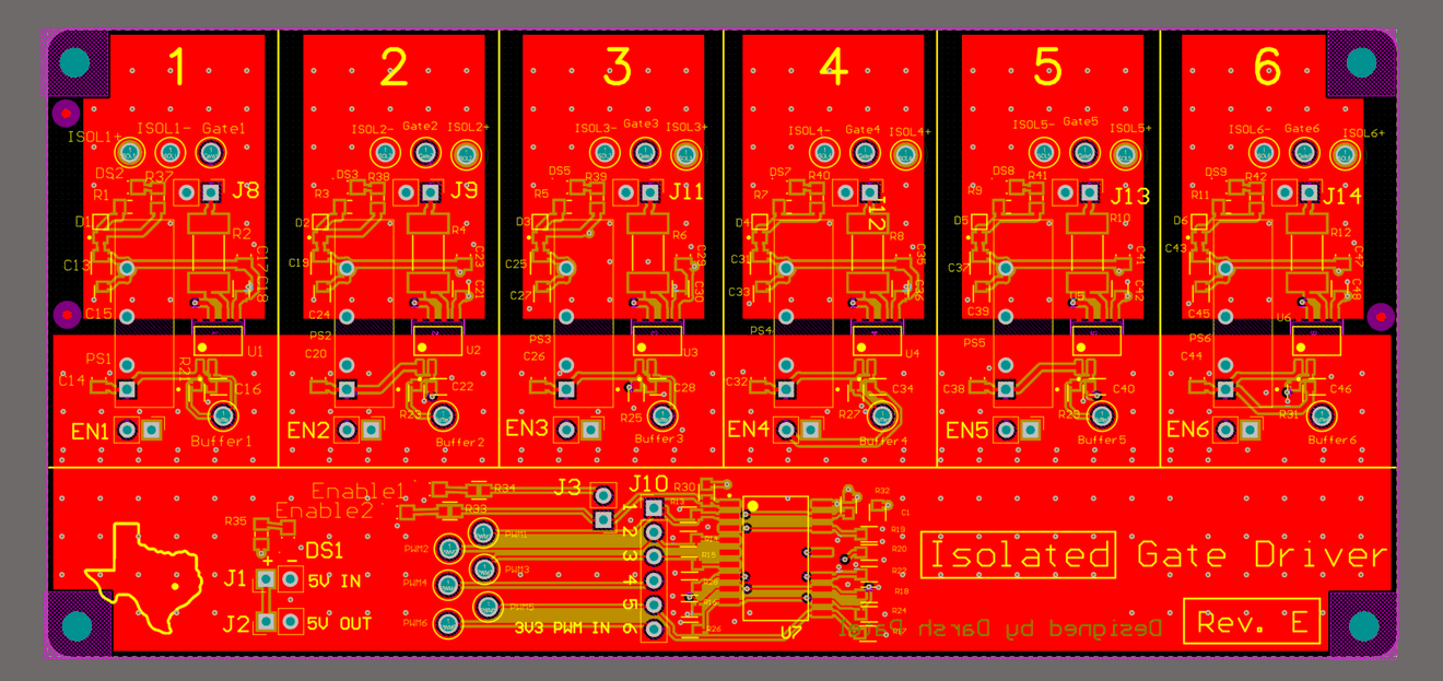
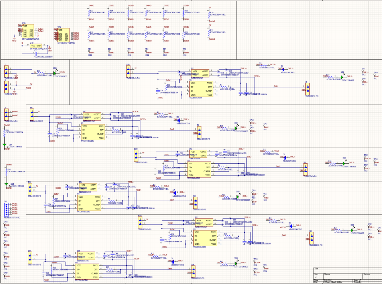
Rev E circuitry and design notes
Six 3.3 V PWM signals go into the board through one header. An SN74AHCT244 buffer changes these signals to 5 V logic for the gate drivers. Header J3 controls the two active-low output-enable inputs of the buffer. Jumpers EN1 to EN6 connect 5 V to the driver and the converter of each channel.
Each output has a series gate resistor that adjusts the switching speed. In the schematic, the active Miller clamp of the driver connects to the gate side of this resistor. Preload resistors put a load on the unregulated converters. Footprints for optional Zener diodes let you limit the bias-rail voltage. You must examine the clamp, the resistor values and the gate wiring with the applicable transistor and switching conditions.
I selected some components only for their PCB footprint, schematic symbol and 3D CAD model. Some catalog values in the schematic are not purchase values. For example, the preload symbols show 75 Ω, but the selected preload is 2 kΩ. The 2512 gate-resistor symbols show 39 kΩ, but the selected value for initial tests is 10 Ω. The repository records these differences and the changes to the header pitch.
Rev D bench test
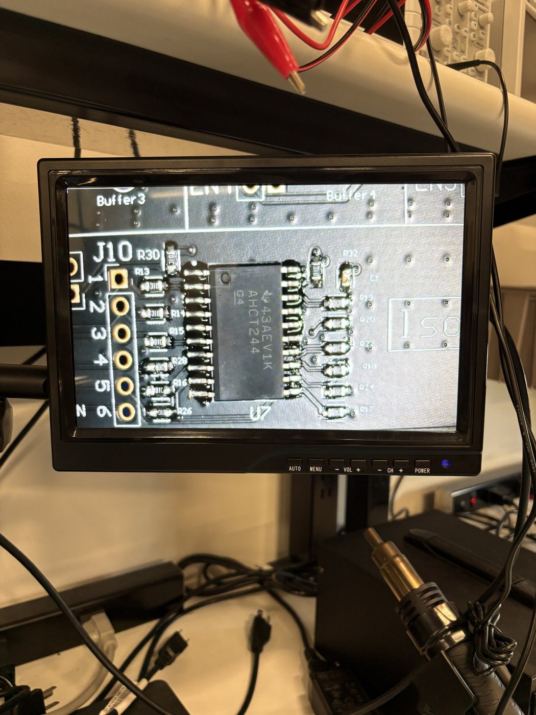
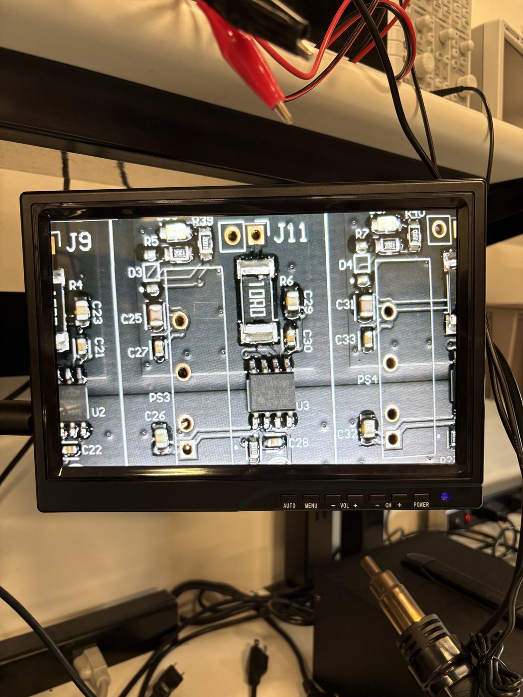
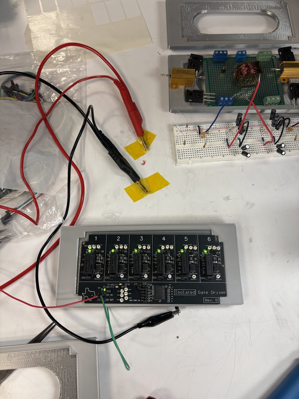
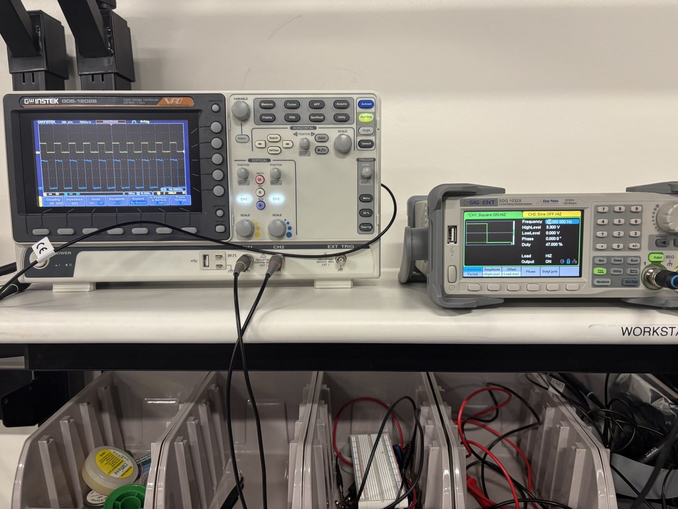
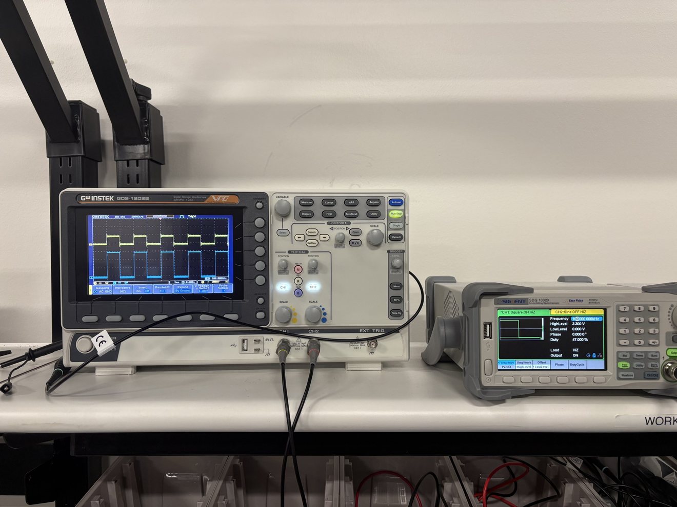
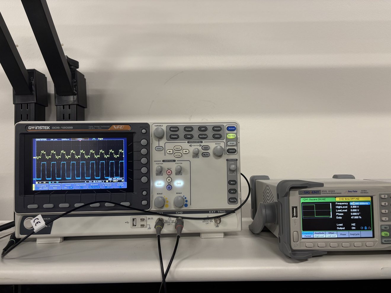
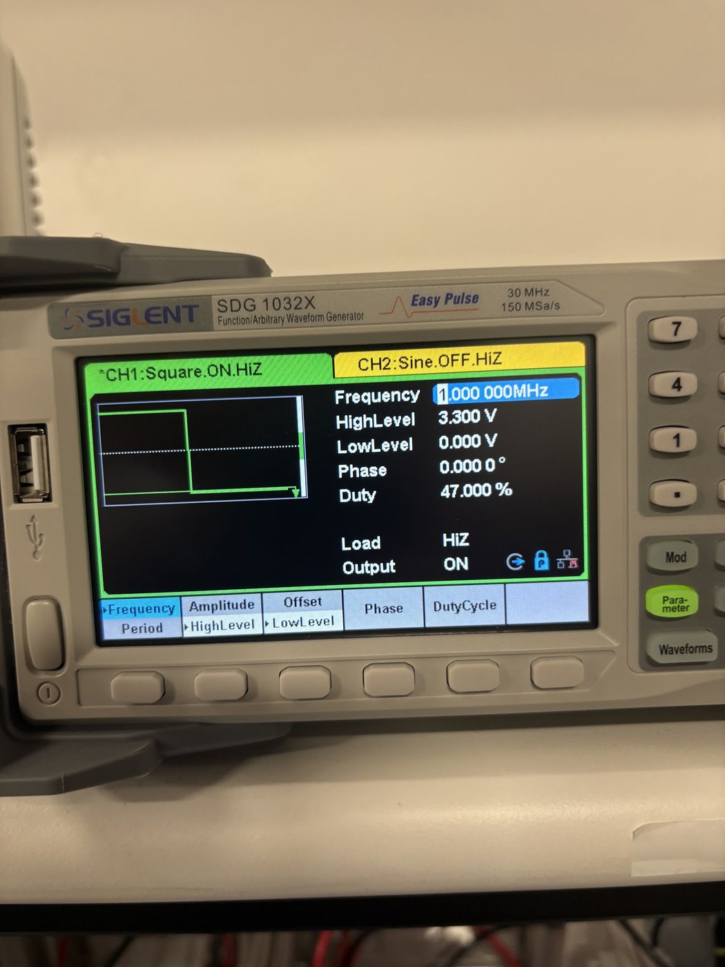
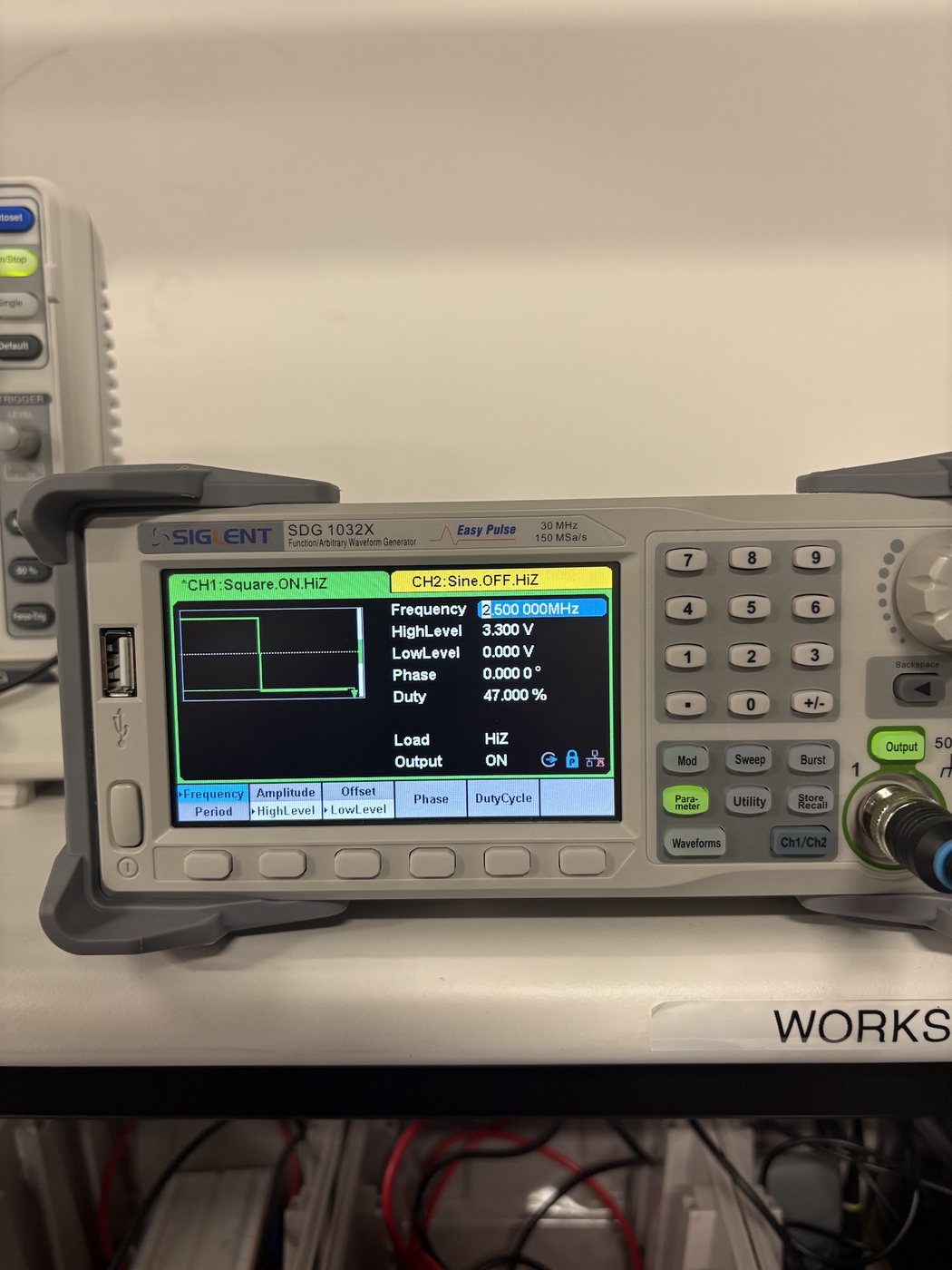
After assembly, I examined the solder joints of the Rev D board with a digital inspection microscope. Then I did a bench test of the board. A function generator replaced the controller. A Siglent SDG1032X supplied a square wave to the PWM input: 3.3 V high, 0 V low and 47% duty cycle. The output of the generator was set for a high-impedance load. The SN74AHCT244 buffer on the board changed this signal to 5 V logic for the driver.
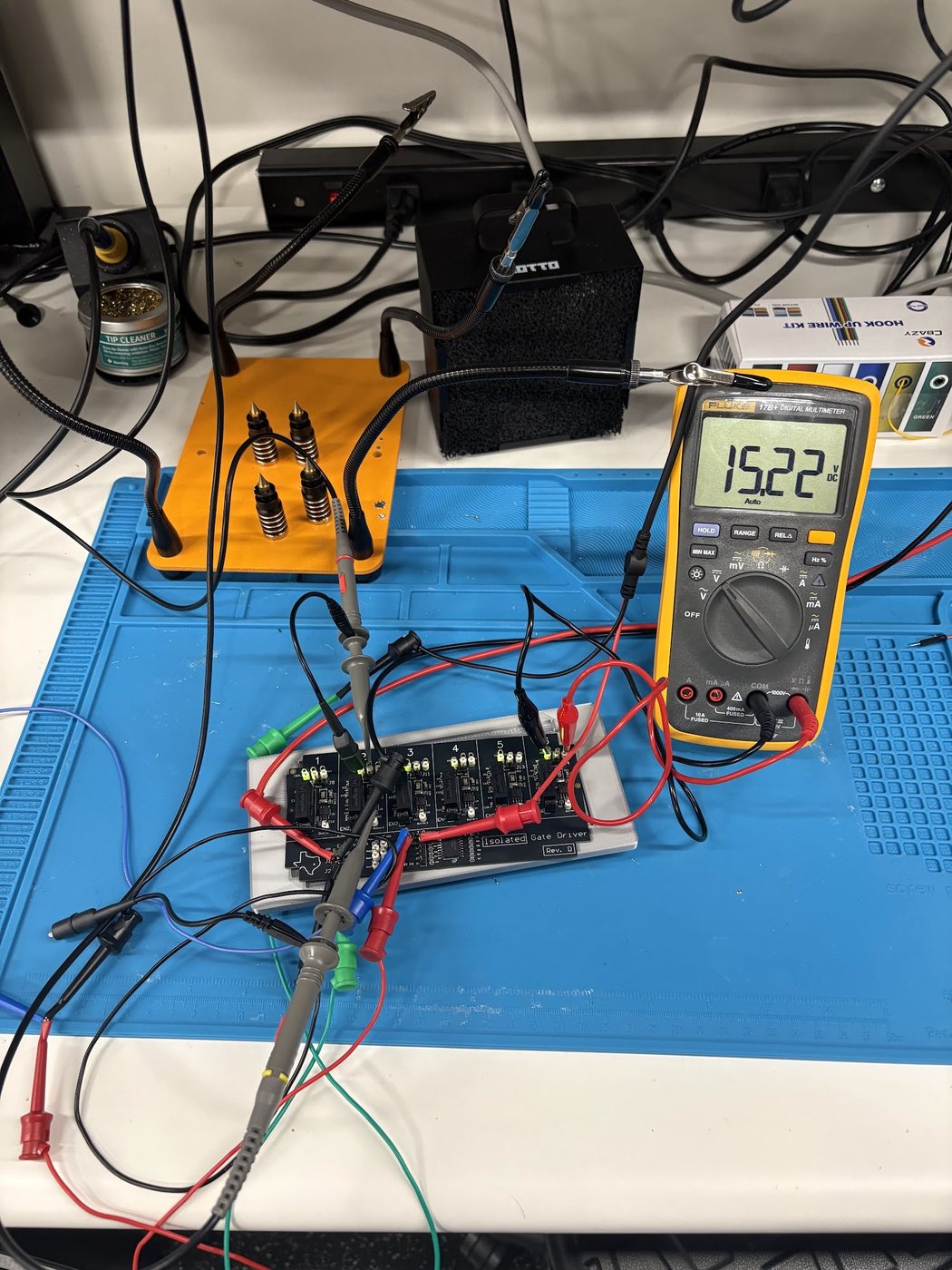
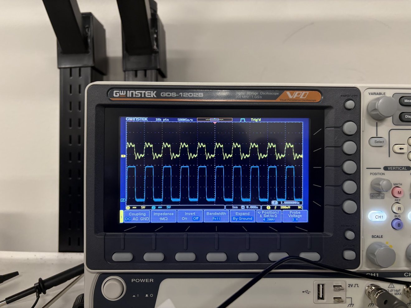
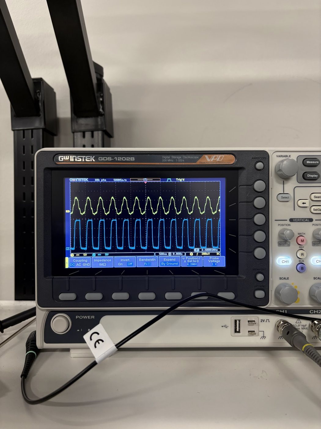
A GW Instek GDS-1202B oscilloscope showed the 5 V buffered signal and the gate output together. I measured the gate output against the isolated return of the channel, not against the control ground.
I did the test at 50 Hz, 100 kHz, 900 kHz, 1 MHz and 2.5 MHz. The gate output followed the input signal correctly at all of these frequencies. During switching, a Fluke meter measured 15.22 V on the isolated rail of the channel. I recommend a maximum operating frequency of 750 kHz.
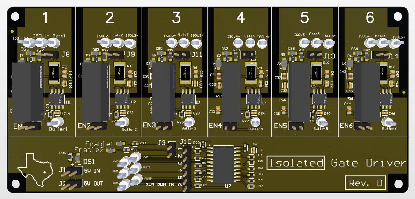
Earlier revisions
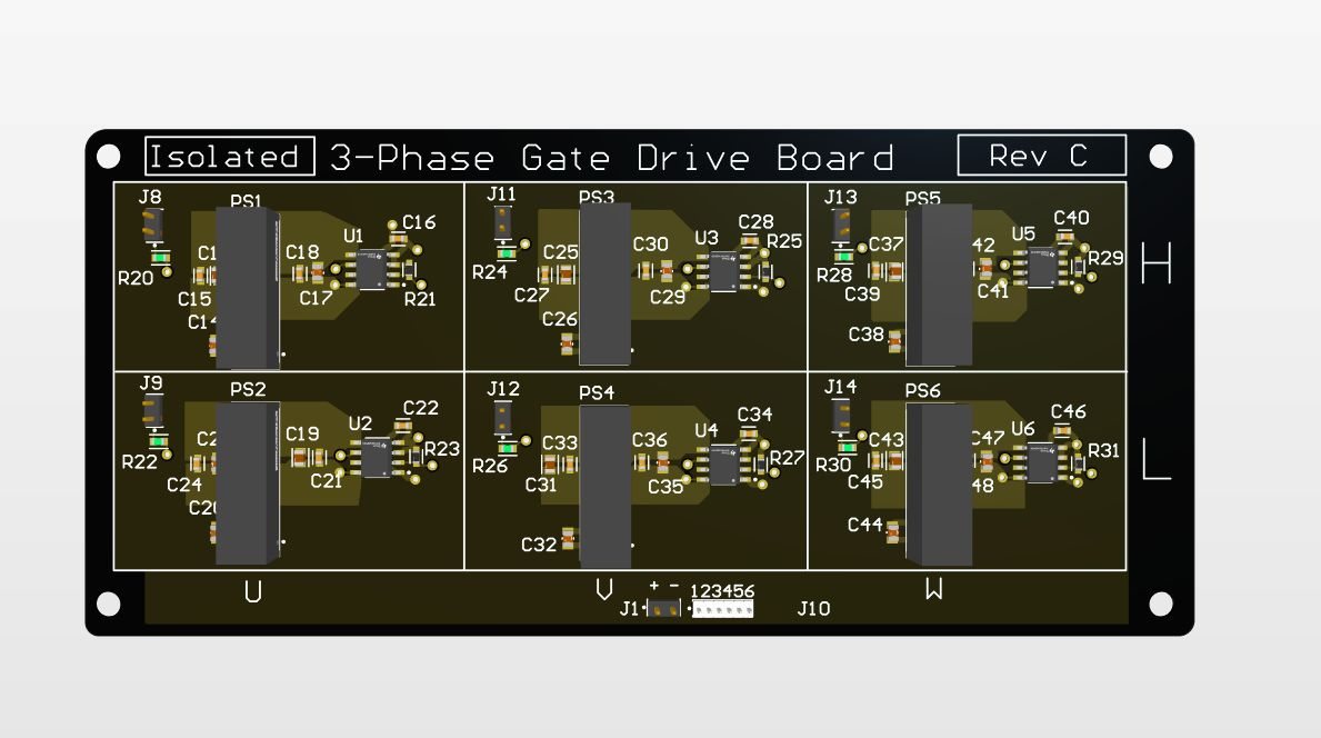
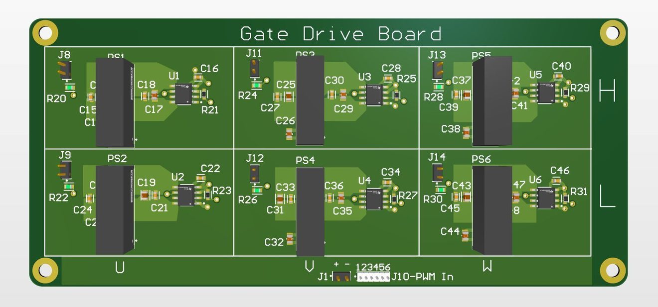
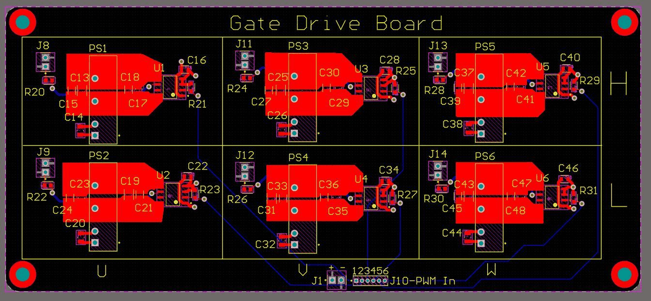
Rev C and Rev B are earlier versions of this board. They are here for reference only.