1 kW dual active bridge
I designed and simulated a 1 kW bidirectional dual active bridge for a 13-series battery pack. The schematic passes ERC and the layout passes DRC. I closed the project before fabrication or hardware tests.
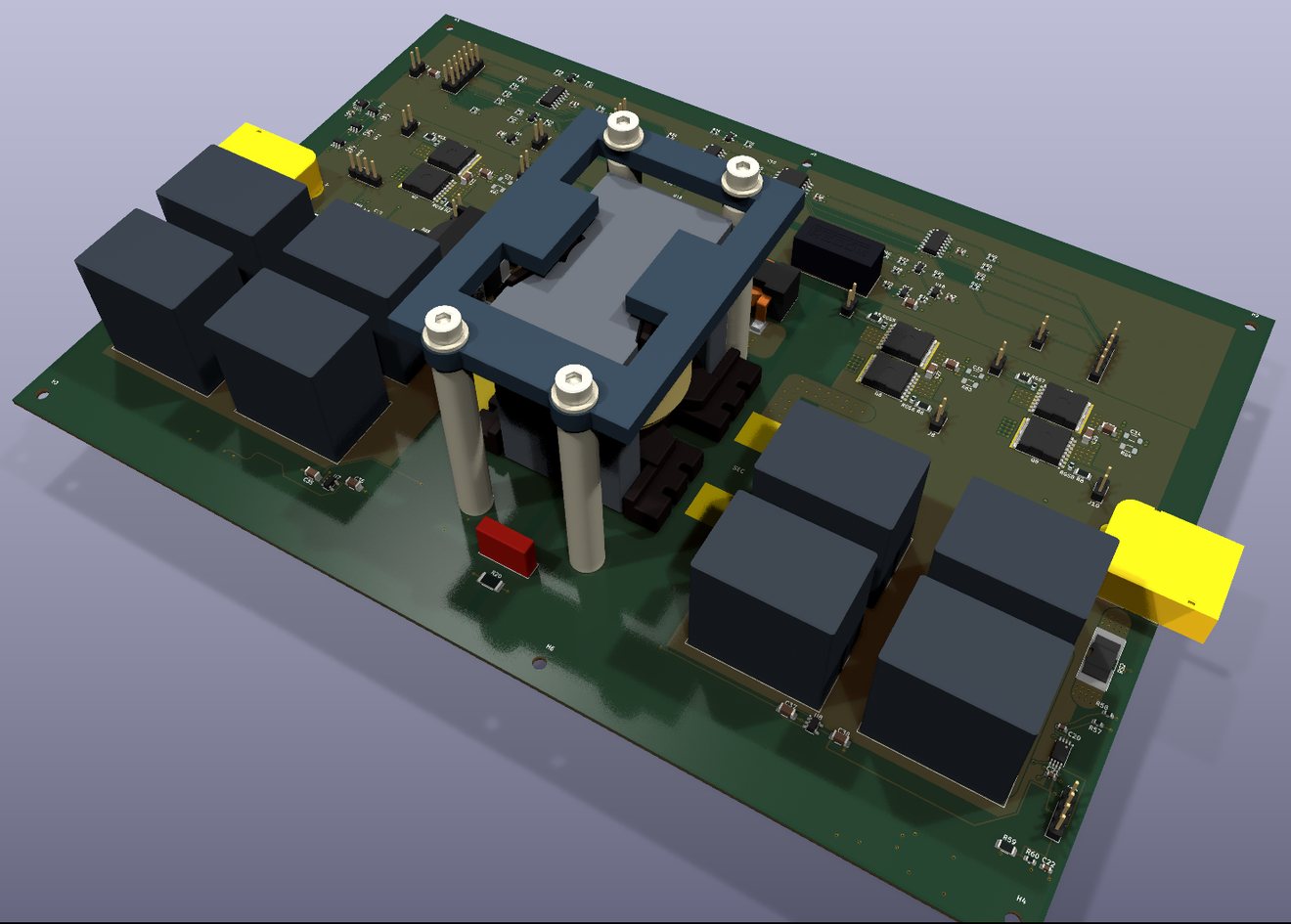
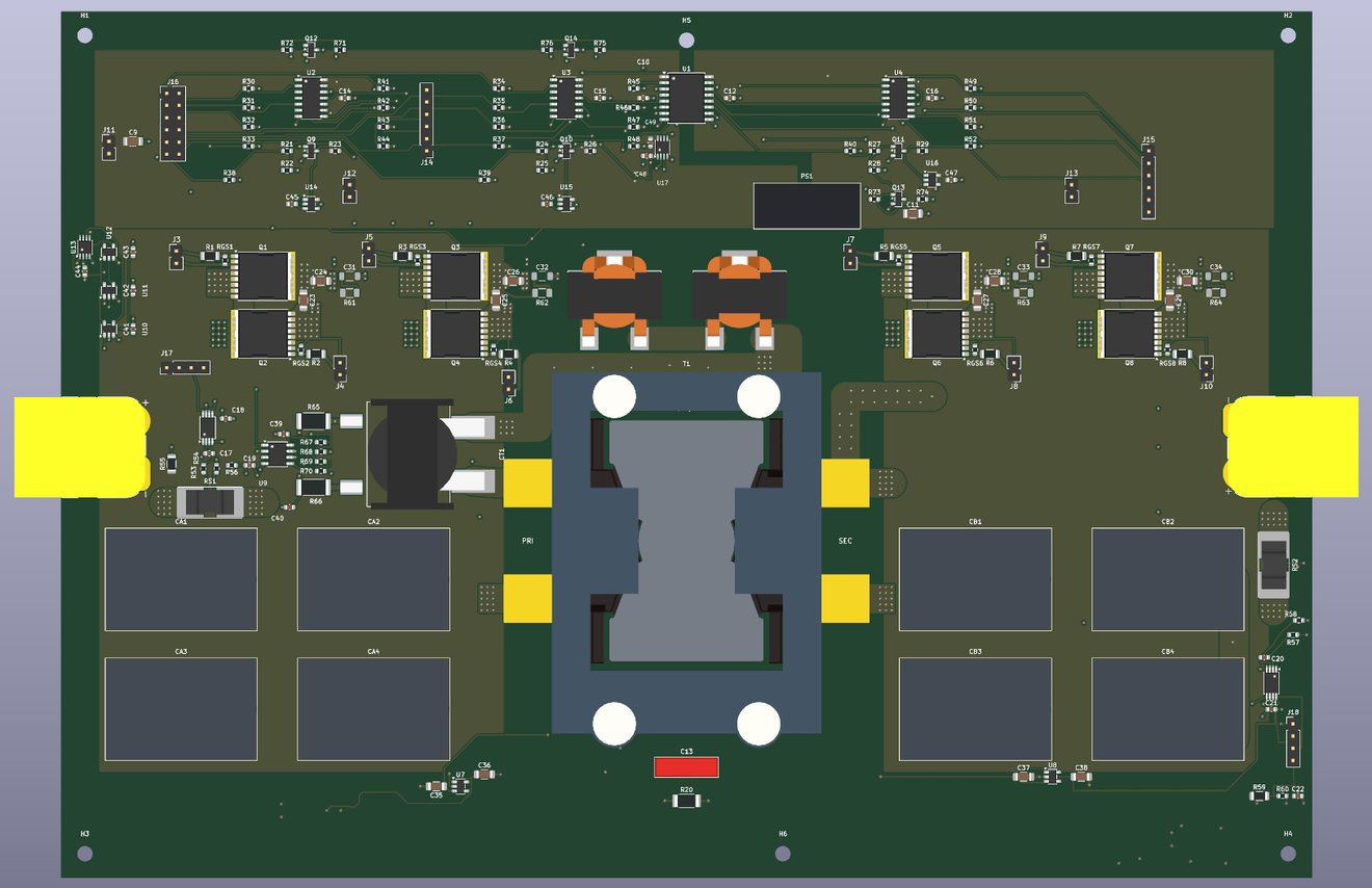
The design switches at 100 kHz between a 48 V source and a 39 to 54.6 V battery. Each full bridge uses four Infineon IPT015N10N5 100 V MOSFETs. A 1:1 transformer and two series Coilcraft SER2011 inductors connect the bridges. Two of my Rev D isolated gate-drive boards drive the MOSFETs.
The four-layer board is 260 × 180 mm and 1.6 mm thick, with 2 oz outer copper and 1 oz inner copper. The simulation results and unfinished checks are listed below.
Magnetics and power path
The transformer has 6 turns on each side. The winding is 0.007 in copper foil on a TDK PQ50/50 core of N87 material, with no air gap. Kapton film insulates the winding: 25 µm between layers, and two layers of 125 µm between the primary and the secondary.
Each SER2011 inductor is 0.60 µH ±20%, with a saturation current of 90 A. The total link inductance, with the transformer leakage, is 1.10 µH to 1.60 µH. Each port has four 47 µF, 100 V film capacitors and an XT90 connector. The design uses external 40 A, 70 V DC fuses.
Sensing and protection
Each port has a 1 mΩ shunt resistor and an INA240A1 amplifier with a gain of 20. A 1:100 current transformer in the link supplies a latched comparator. At a nominal 49.85 A, the comparator trips and pulls all the gates low. Each isolated domain has its own 3.3 V regulator.
Each Rev D gate-driver board has six UCC5310 drivers, 10 Ω gate resistors and isolated DC-DC modules. The gate-drive voltage is 15 V. The dead time is not set: a 200 ns dead time failed the simulation check.
Simulation results
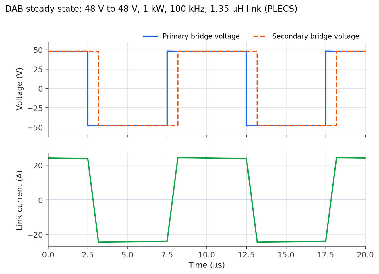
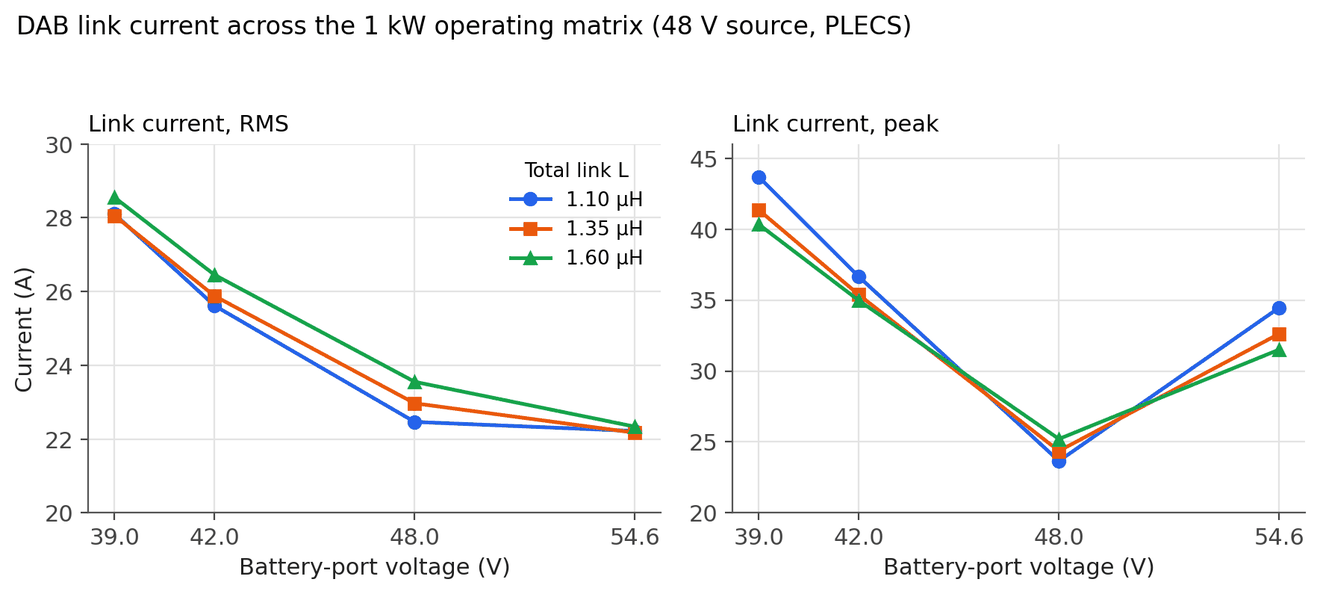
I simulated the converter in PLECS at 1 kW. The sweep used battery voltages of 39 V, 42 V, 48 V and 54.6 V, and link inductances of 1.10 µH, 1.35 µH and 1.60 µH.
| Result (worst case of the sweep) | Value |
|---|---|
| Link current | 28.554 A RMS, 43.680 A peak |
| Input capacitor current | 19.308 A RMS |
| Output capacitor current | 12.942 A RMS |
| MOSFET conduction loss, both bridges | 4.894 W at 1.5 mΩ, 10.762 W at 3.3 mΩ (hot) |
| Heatsink requirement | 6.9 K/W or less, for a 125 °C junction at 50 °C ambient |
At all 960 switching edges, the current had the correct direction for zero-voltage switching (ZVS). This result does not prove ZVS. I did not calculate the switching loss or the efficiency.
Open items when the work stopped
These items were not complete: the extraction of the switching-loop inductance, the current and thermal checks, the cooling design and the heatsink mounting holes. The test points, the indicator LEDs, the port disconnect switches and the final fabrication files were also not complete. A layout review on 8 October 2026 found signal and power traces in the two inner ground planes.